
A Deep Dive into AI Chip Architectures
GPUs, NPUs, Photonics, and more..

There’s a fascinating hardware landscape evolving beneath our AI workloads, and it’s worth understanding what makes each approach unique. While we often think about model architectures and training techniques, the chip designs running these computations have their own compelling engineering tradeoffs and innovations.
Let’s explore what’s powering AI systems today and what’s on the horizon..
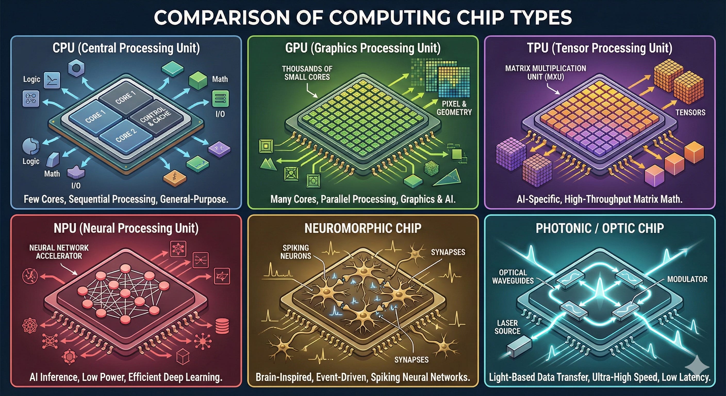
Before we start, I asked Nano Banana to create this summary image to help illustrate differences in chips. At a high level, it’s impressive, given how little it had to go on. But let’s dig a bit deeper..
The Chips We’re Using Right Now…
GPUs: The Parallel Processing Powerhouses
GPUs dominate the AI training landscape, and their architecture reveals why they’re so effective for neural network workloads.
GPUs were originally built to render graphics, which turns out to require doing the same operation on tons of data points simultaneously. Sound familiar? That’s exactly what matrix multiplication needs. The architecture is built around thousands of smaller cores working in parallel, which makes them fantastic for the embarrassingly parallel workloads in deep learning.
The thing is, GPUs are generalists by design. They can run training jobs, render graphics, or process scientific simulations. This flexibility means they’re not maximally optimized for any single workload, but the mature ecosystem (particularly NVIDIA’s CUDA platform) and their proven ability to handle diverse operations make them incredibly valuable.
TPUs: Google’s Secret Sauce
Tensor Processing Units are Google’s answer to “what if we built chips specifically for neural networks?” Unlike GPUs, TPUs were designed from the ground up for tensor operations. They use a systolic array architecture, which is basically a clever way of moving data through a grid of processors so that each piece of data gets reused multiple times without hitting memory.
The big win with TPUs is efficiency. They’re optimized for the specific matrix operations in neural networks, particularly inference. Google uses them extensively for their own models and makes them available through Google Cloud, though the ecosystem isn’t nearly as mature as NVIDIA’s.
One quirk: TPUs are really, really good at what they do, but they’re less flexible than GPUs. If your model doesn’t map well to their architecture, you might not see the speedups you’re hoping for.
CPUs: The Flexible Foundation
CPUs continue to play a role in AI workloads, particularly for inference in production environments. Intel’s Xeon processors and AMD’s EPYC chips serve smaller models and situations requiring flexibility.
The advantage is ubiquity and maturity. CPUs are everywhere, the tooling is battle-tested, and they handle diverse workloads seamlessly. Modern CPUs have added specialized instruction sets (like Intel’s AVX-512 or AMX) to better support AI operations, though they remain fundamentally designed for sequential processing rather than the massive parallelism AI demands.
NPUs: Specialized Accelerators for Inference
Neural Processing Units represent a growing category of specialized accelerators, particularly prevalent in edge devices. Recent smartphones and laptops increasingly include dedicated NPUs for on-device AI inference.
NPUs are typically much smaller and lower power than GPUs or TPUs, optimized for running already-trained models rather than training new ones. They’re perfect for running a voice assistant or processing images on your phone without killing the battery or sending everything to the cloud.
In the data center context, you’re seeing NPU-like architectures from companies like Cerebras and Groq, which take the specialization concept to the extreme with wafer-scale chips or custom architectures designed to eliminate memory bottlenecks.
Future Directions: Emerging Chip Tech…
Neuromorphic Chips: Event-Driven Computing
Neuromorphic chips take inspiration from biological neural networks, implementing event-driven, asynchronous processing. Intel’s Loihi and IBM’s TrueNorth exemplify this approach, using spiking neural networks rather than the continuous activation functions we typically use in deep learning.
The potential lies in energy efficiency. Biological neurons operate with remarkable power efficiency, and neuromorphic chips aim to capture some of those advantages. The challenge is that current deep learning frameworks and model architectures don’t directly map to neuromorphic substrates (running a standard transformer on a neuromorphic chip would require fundamental rethinking of the model itself). These chips show promise for specific pattern recognition and sensory processing tasks, but adapting them for large-scale models remains an open research question.
Key resources for neuromorphic computing:
Intel Loihi 2 paper - Foundational architecture paper
Open Neuromorphic community - Comprehensive resource with hardware guides and tutorials
IBM TrueNorth design paper - Details on the 1M neuron chip
Intel’s Neuromorphic Research Community - Access to Loihi systems and publications
Hala Point system announcement - 1.15 billion neuron neuromorphic system
Photonic and Optical Chips: Computing with Light
Photonic computing represents a fundamentally different approach to computation. Companies like Lightmatter and Luminous Computing are developing chips that perform matrix multiplication using optical interference patterns rather than electronic transistors.
The appeal comes from three key advantages: speed (light travels faster than electrons in circuits), energy efficiency (certain optical operations require less energy than their electronic equivalents), and reduced heat generation. Matrix multiplication, the core operation in neural network inference, maps particularly well to optical computing techniques.
Current implementations tend toward hybrid architectures, where optical components handle specific operations while electronic components manage control logic and memory operations. The manufacturing processes differ significantly from traditional semiconductor fabrication, and building mature ecosystems around these technologies remains a significant challenge. Early commercial products are emerging, though widespread adoption likely remains several years away as the technology matures and manufacturing scales up.
Key resources for photonic computing:
Lightmatter’s Nature paper (2025) - Demonstrates photonic processor running ResNet and BERT with near-electronic precision
Lightmatter Passage M1000 announcement - 114 Tbps photonic interconnect chip
Hot Chips 2025 presentation on Passage M1000 - Technical deep dive
MIT News on Lightmatter - Accessible overview of photonic computing
Luminous Computing overview - Another major player in photonic AI acceleration
The Current State and What’s Ahead
Large model training today predominantly happens on GPUs (particularly NVIDIA’s offerings) or TPUs for those working within Google’s ecosystem. This configuration has proven reliable and well-supported, with mature tooling and established workflows.
The inference landscape shows more diversity. While GPUs continue to dominate for serving large models, specialized chips from companies like Groq and Cerebras are gaining traction for high-throughput inference workloads. Edge deployment increasingly leverages NPUs for efficient on-device inference.
Resources on specialized inference chips:
Groq LPU architecture - Details on their Language Processing Unit design
Groq technical deep dive - Comprehensive breakdown of the Tensor Streaming Processor
Cerebras WSE-3 announcement - World’s largest chip with 4 trillion transistors
Cerebras vs NVIDIA comparison paper - Academic analysis of wafer-scale technology
UC Riverside wafer-scale study - Sustainability and efficiency analysis
Neuromorphic and photonic technologies remain in earlier stages of development. They’re advancing steadily and offer intriguing possibilities for energy efficiency and performance, but they require ecosystem development and proof of scalability before they’ll reshape production AI systems. The progress in these areas is worth watching - as models grow and inference costs scale, the efficiency advantages these technologies promise could become increasingly important.
The chip architectures running our models involve fascinating engineering tradeoffs between specialization and flexibility, performance and power efficiency, maturity and innovation. Understanding these tradeoffs helps contextualize both current capabilities and future possibilities in AI systems.
Additional Resources
General chip architecture:
Google TPU paper series - TPU v2-v5 system architectures
NVIDIA H100 architecture whitepaper - Latest Hopper GPU details
Intel’s AI accelerator portfolio - Including Gaudi and data center GPU
For staying current:
Hot Chips conference proceedings - Annual symposium on high-performance chips
ISCA (International Symposium on Computer Architecture) - Leading venue for architecture research
arXiv cs.AR section - Preprints in computer architecture
As always, all opinions are my own and do not reflect any employer or funding agency.
Fantastic overview of the hardware landscape underlying modern AI systems. The section on photonic computing is particularly compelling because it highlights a paradigm where the physics of light naturally aligns with matrix multiplication operations. What often gets overlooked is that the hybrid architecture approach these companies are taking might actually be the more sustainable path forward than pure optical systems, since it lets teams iterate on the optics while leveraging existing CMOS toolchains for everything else. The question of whether photonic interconnects will find their first killer app in datacenter networking before computation is an intereting one to watch.